Scanning Tunneling Microscope
The scanning tunneling microscope (not to be confused with scanning electron microscopes), or STM, is the most powerful type of microscope ever built. It was invented in 1981 by Gerd Binnig and Heinrich Rohrer of IBM's Zurich Lab in Zurich, Switzerland. The invention garnered the two a Nobel prize for physics in 1986. The STM allows scientists to see and position individual atoms, with higher resolution than its related cousin, the atomic force microscope. Both the STM and the AFM fall under the class of scanning probe microscopy instruments.
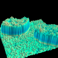
It is used to obtain images of conductive surfaces at an atomic scale ~2 Å (2 x 10⁻¹⁰ m or 0.2 nm). It can also be used to alter the observed material by manipulating individual atoms, triggering chemical reactions, and creating ions by removing individual electrons from atoms and then reverting them to atoms by replacing the electrons.
Overview
The STM is a non-optical microscope which employs principles of quantum mechanics. A very fine probe is moved over the surface of the material under study, and a voltage is applied between probe and the surface. Depending on the voltage and its characteristics electrons will "tunnel" (this is a quantum-mechanical effect) or jump from the probe to the surface (or vice-versa depending on the polarity), resulting in a weak electric current. The size of this current is exponentially dependent on the distance between probe and the surface. Obviously, for a current to occur the substrate being scanned must be conductive. Insulators can not be scanned through the STM. By scanning the probe over the surface and measuring the current, one can thus reconstruct the surface structure of the material under study. Adjustments of the distance between probe and surface are done using a servo loop and converse piezoelectricity.
Use of the STM
Far from simply a fancy microscope, the STM offers much in the way of surface science studies. Conduction mechanisms can be studied by analyzing a substrate via scanning tunneling spectroscopy, or STS, which is when the feedback loop is momentarily interrupted during a scan to obtain dI/dV (point conductance) measurements. Furthermore, the STM can be used to study charge transport mechanisms in molecules, surface domain formations in self-assembled monolayers and Langmuir-Blodgett films, defect sites in molecules and substrates, and so forth. STM is particularly useful in nanoscale chemistry labs, where the study of defects and physical structure of synthetic chemical compounds is of vital importance.
Reading and References
1- Introduction to Scanning Tunneling Microscopy
All text is available under the terms of the GNU Free Documentation License. See Wikipedia for details.
Nanotechnology Resources
- Atomic Force Microscope
- Nanomedicine
- Mechanosynthesis
- Molecular Assembler
- Molecular Engineering
- Graphene Applications
- Molecular Nanotechnology
- Nanorobotics
- What is a Nanometer?
- What is a Nanocar?
- Scanning Tunneling Microscope
- Self Assembly
- Supramolecular Chemistry
- The carbon molecule
- Buckyball -- Fullerene